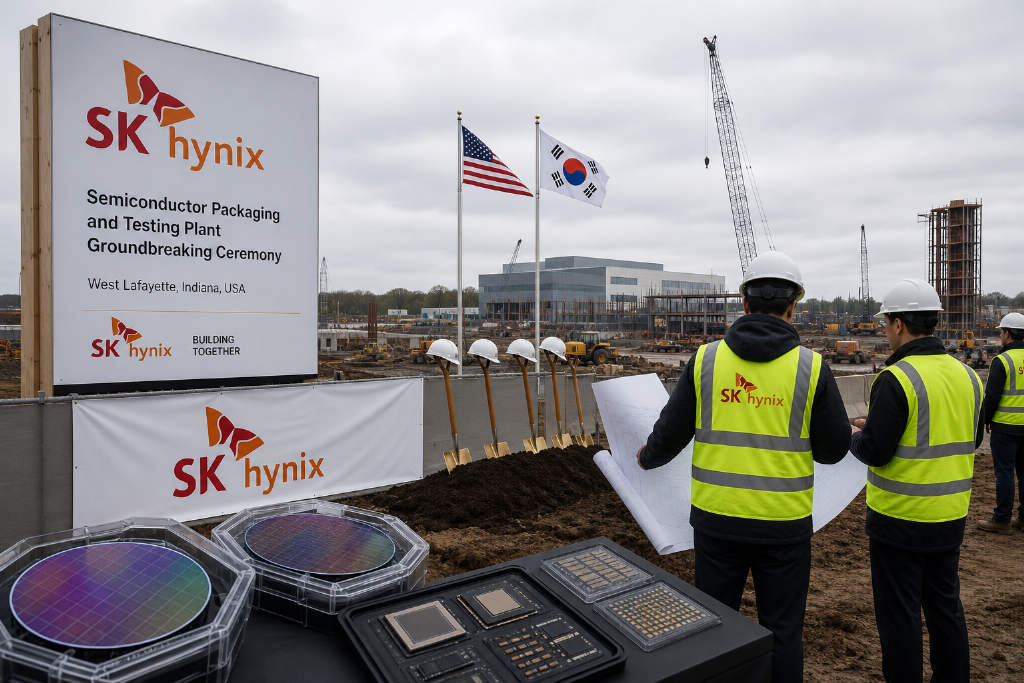
SK hynix2026-08-28 02:18:55SK hynix breaks ground in Indiana for next-generation HBM packaging and testing baseSK hynix held a groundbreaking ceremony on Aug. 27 in Indiana for an advanced packaging artificial intelligence wafer facility, a project the company said will involve more than $4 billion in investment. The site is intended to become the first U.S. production base for high bandwidth memory, or HBM, and will serve as a key link in semiconductor cooperation between South Korea and the United States. Under the operating plan, advanced wafers made in South Korea will be shipped to Indiana for advanced packaging and testing before being delivered to U.S. customers as products made in America. The company said the cleanroom is scheduled to open in October 2028, with mass production of next-generation HBM set for the second half of 2029. The facility is expected to hire about 1,000 professionals across technical and operational roles, while the broader project and follow-on business activity are estimated to create about 7,000 direct and indirect jobs locally and across the U.S. SK hynix also signed an MOU with Purdue University on joint research covering system integration and advanced packaging technologies, including HBM.1330